Hardware
This section details the electrical aspects and interfaces of the iW-DigitalAmplifier (Rev. RV01), based on the product datasheet.
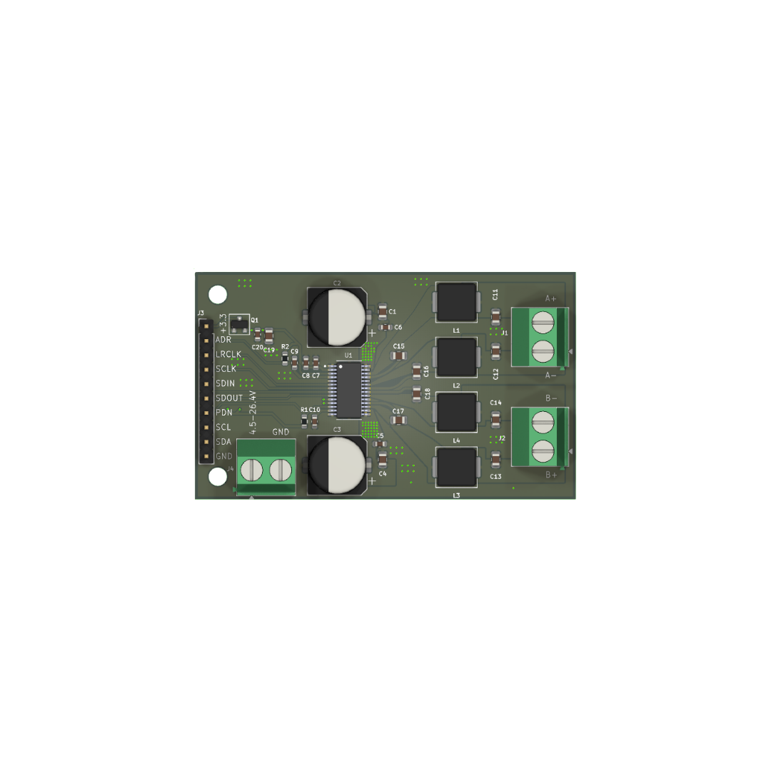
Board overview
The iW-DigitalAmplifier is a digital-audio breakout board built around the TAS5805M (Texas Instruments), a digital-input Class-D stereo amplifier with an integrated audio processor. It exposes the power supply (PVDD) on a screw terminal, the audio and control signals on a 10-way connector, and the speaker outputs on dedicated terminals, with the output LC filters already integrated.
3D model
Drag to rotate, scroll to zoom.
Main features
TAS5805Mamplifier, closed-loop Class-D stereo, digital input- power of 2 x 23 W (8 ohms, 21 V) stereo, up to 45 W in mono mode (4 ohms)
- I2S / TDM audio input (LRCLK, SCLK, SDIN, SDOUT)
- I2C control (SCL/SDA), address selectable via ADR/FAULT
- integrated 96 kHz DSP: SRC, 15 biquads per channel, 3-band DRC and AGL
- PVDD supply from 4.5 V to 26.4 V via screw terminal
- integrated LC output filter (10 uH + 0.68 uF per line)
- stereo bridge (BTL) outputs on OUT_A / OUT_B terminals
- 3.3 V switch via
AO3401AP-MOSFET and a FAULT protection pin - 2 M3 mounting holes
Electrical specifications
| Parameter | Min. | Typ. | Max. | Unit / Notes |
|---|---|---|---|---|
| Supply voltage (PVDD) | 4.5 | 12 – 21 | 26.4 | V — J4 terminal |
| System logic voltage | — | 3.3 | — | V — internal rail |
| Stereo output power (2.0) | — | 2 x 23 | — | W — 8 ohms, 21 V, THD+N = 1% |
| Mono output power | — | 45 | — | W — 4 ohms, 21 V, THD+N = 1% |
| THD+N | — | ≤ 0.03 | — | % — 1 W, 1 kHz, PVDD = 12 V |
| SNR (A-weighted) | 107 | — | — | dB |
| Quiescent current | — | 16.5 | — | mA — PVDD = 13.5 V |
| DSP sample rate | — | 96 | — | kHz |
| PWM switching frequency | — | 384 / 768 | — | kHz — configurable |
| Operating temperature | -25 | — | +85 | °C |
Power, THD+N and SNR figures per the TAS5805M datasheet (Texas Instruments). Actual power depends on the applied PVDD voltage, the speaker impedance and the assembly's thermal dissipation.
Power management
The board has two power domains. The power (PVDD) enters through the J4 terminal, passes through a 600-ohm ferrite bead (FB1) and a capacitor bank that feeds the Class-D output stages. The 3.3 V logic powers the digital and analog sections of the TAS5805M (DVDD, AVDD, VR_DIG), switched by an AO3401A P-MOSFET.
| Resource | Description |
|---|---|
| Power input | PVDD 4.5-26.4 V on the J4 terminal (2-way screw terminal) |
| PVDD filtering | C2/C3 390 uF + C1/C4 22 uF + C5/C6 100 nF; FB1 ferrite 600 ohms |
| 3.3 V rail | AO3401A P-MOSFET switch (Q1) with C19 10 uF / C20 100 nF |
| IC domains | DVDD, AVDD and VR_DIG with C9/C10 1 uF decoupling |
| Control / protection | PDN pin (power-down) and ADR/FAULT with pull-ups |
Interfaces and output stage
Digital audio input — I2S
An I2S / TDM serial interface for the audio stream: LRCLK (word clock), SCLK (bit clock), SDIN (input data) and SDOUT (loopback/TDM). Compatible with microcontrollers, DACs and SoCs with I2S output.
Control — I2C
The TAS5805M is configured over I2C (SCL/SDA, with 10 k pull-ups). The device address is set by the ADR/FAULT pin, which also signals faults (overcurrent, over-temperature, clipping). The PDN pin controls power-down mode.
Output stage and LC filter
Each channel drives a bridge (BTL) output: OUT_A and OUT_B. Before the terminals, each line passes through an LC filter (10 uH inductor + 0.68 uF capacitor), reducing EMI and delivering clean audio to the J1 and J2 speaker terminals.
Audio and control connector (J3, 1x10)
The J3 connector brings together the digital audio (I2S) signals, the control bus (I2C) and the TAS5805M management signals, plus the reference ground.
| Pin | Signal | Type | Function | Notes |
|---|---|---|---|---|
| 1 | ADR/FAULT | I/O | I2C address selection / fault | R2 pull-up 15 k |
| 2 | LRCLK | input | I2S word clock | L/R sync |
| 3 | SCLK | input | I2S bit clock | — |
| 4 | SDIN | input | digital audio data (I2S) | input stream |
| 5 | SDOUT | output | audio data (loopback / TDM) | — |
| 6 | PDN | input | power-down (active low) | R1 pull-up 10 k |
| 7 | SCL | input | I2C bus clock | R3 pull-up 10 k |
| 8 | SDA | I/O | I2C bus data | R4 pull-up 10 k |
| 9 | GND | power | reference / ground | — |
| 10 | GND | power | reference / ground | — |
The I2S and I2C signals operate at a 3.3 V logic level. The ADR/FAULT pin sets the TAS5805M I2C address and reports the amplifier's fault conditions.
Online schematic
View the hardware project directly in your browser:
Mechanical and environmental information
| Item | Specification |
|---|---|
| Power terminal | J4 — 2-way screw terminal (PVDD / GND) |
| Audio/control connector | J3 — 1x10 header (I2S + I2C + GND) |
| Output terminals | J1 (Channel A) and J2 (Channel B) — 2-way screw terminals |
| Mounting holes | 2 x M3 mounting holes |
| Thermal dissipation | TAS5805M PowerPAD to the copper plane |
| Operating temperature | -25 °C to +85 °C |
| Logic voltage | 3.3 V |