Hardware
This section details the physical and electrical aspects of the iW-CORE-BOARD-V1 (Rev. RV01), based on the product datasheet.
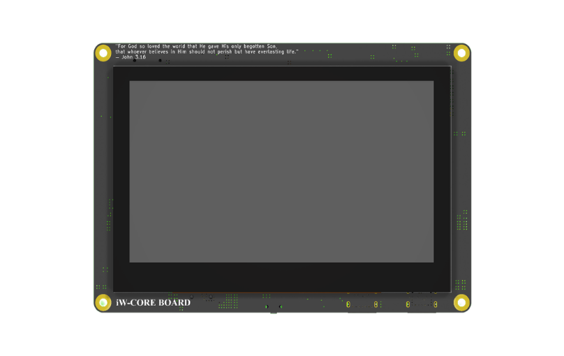
Board overview
The iW-CORE-BOARD-V1 is a core board and HMI platform built around the STM32H7 (Cortex-M7 up to 480 MHz). It integrates a display, wireless connectivity, power and expansion to act as the processing core for a family of application boards (shields).
3D model
Drag to rotate, scroll to zoom.
Main features
STM32H743VIT6(2 MB Flash) orSTM32H750VB(128 KB + external flash) MCU- 1 MB of internal SRAM (incl. DTCM/ITCM)
- 4.3" TFT display with 480x272 and capacitive touch
- Wi-Fi 802.11 b/g/n + BLE via the
Quectel FC41Dmodule - 3-axis accelerometer over I2C
IP5306PMIC (Li-ion charging, boost and power on/off via button)BL-5Cmain battery andCR1220RTC backup- USB Full Speed (OTG) + USB-Serial for console/log
- SD/microSD card reader (SDMMC)
- two
iW-APPLICATIONexpansion connectors (J4 and J5) - compatible with
LVGLandTouchGFX
Electrical specifications
| Parameter | Min. | Typ. | Max. | Unit / Notes |
|---|---|---|---|---|
| USB input voltage (V_BUS) | 4.5 | 5.0 | 5.5 | V — USB connector |
| Battery voltage (BL-5C, Li-ion) | 3.0 | 3.7 | 4.2 | V — single cell |
| System logic voltage | — | 3.3 | — | V |
| RTC backup battery (CR1220) | — | 3.0 | — | V — coin cell |
| CPU clock frequency | — | — | 480 | MHz (Cortex-M7) |
| Display resolution | — | 480x272 | — | pixels (4.3") |
| Battery charge current | — | — | ~2.0 | A — IP5306 (typical) |
| Operating temperature | -40 | — | +85 | °C — limited by the components |
Consumption depends on firmware, display brightness, RF power and active peripherals. The charge current is set by the IP5306 and the BL-5C battery capacity.
Power management (PMIC IP5306)
The power circuit revolves around the IP5306, a power-bank-type IC that integrates a Li-ion charger, a 5 V boost converter and on/off button control.
| Resource | Description |
|---|---|
| Power inputs | USB (5 V) and BL-5C Li-ion battery |
| Charging | integrated Li-ion charger with status indication |
| Output | 5 V boost and the system's 3.3 V rail |
| ON/OFF control | power on/off via a button managed by the IP5306 |
| RTC backup | CR1220 coin cell keeps the real-time clock running |
Integrated peripherals
4.3" TFT display with capacitive touch
A 480x272 color panel driven by the parallel RGB interface (STM32H7 LTDC controller), with capacitive touch read over I2C. It supports accelerated graphics rendering with LVGL and TouchGFX.
Connectivity — Quectel FC41D
Wi-Fi 802.11 b/g/n and BLE at 2.4 GHz, enabling network connection, provisioning, OTA and communication with apps and cloud.
3-axis accelerometer
An inertial sensor over I2C for motion detection, screen orientation, gestures and power saving.
Storage — SD card
An SD/microSD reader over SDMMC for logs, graphic assets (fonts, images), configurations and application data.
USB and USB-Serial
The STM32H7's USB Full Speed (OTG) port plus a dedicated USB-Serial converter for console, debugging and firmware flashing.
iW-APPLICATION expansion connectors (J4 and J5)
The board exposes the STM32H7 GPIOs on two 2x9 connectors (18 ways). Most pins are multifunction; the alternate functions refer to the STM32H743VIT6 (LQFP100). The J5 analog pins serve as ADC inputs.
Connector J4
| Pin | Signal | Alternate functions | Notes |
|---|---|---|---|
| J4-1 | PE0 | TIM4_ETR, UART8_RX, FMC | general-purpose GPIO |
| J4-2 | PE1 | UART8_TX, FMC | general-purpose GPIO |
| J4-3 | PD5 | USART2_TX, FMC_NWE | UART2 TX |
| J4-4 | PD7 | USART2_CK, SPI1_MOSI | general-purpose GPIO |
| J4-5 | PD2 | SDMMC1_CMD, UART5_RX, TIM3_ETR | general-purpose GPIO |
| J4-6 | PD4 | USART2_RTS, FMC_NOE | general-purpose GPIO |
| J4-7 | PD0 | UART4_RX, FDCAN1_RX, FMC_D2 | general-purpose GPIO |
| J4-8 | PD1 | UART4_TX, FDCAN1_TX, FMC_D3 | general-purpose GPIO |
| J4-9 | PC11 | SDMMC1_D3, USART3_RX, SPI3_MISO | general-purpose GPIO |
| J4-10 | PC12 | SDMMC1_CK, UART5_TX, SPI3_MOSI | general-purpose GPIO |
| J4-11 | PA15 | SPI1/SPI3_NSS, TIM2_CH1, JTDI | general-purpose GPIO |
| J4-12 | PC10 | SDMMC1_D2, USART3_TX, SPI3_SCK | general-purpose GPIO |
| J4-13 | I2C3_SDA | I2C3 bus data (PC9) | I2C3 bus |
| J4-14 | I2C3_SCL | I2C3 bus clock (PA8) | I2C3 bus |
| J4-15 | 3V3 | — | regulated 3.3 V output |
| J4-16 | PC8 | SDMMC1_D0, USART6_CK, TIM3_CH3 | general-purpose GPIO |
| J4-17 | GND | — | reference / ground |
| J4-18 | 3V3 | — | regulated 3.3 V output |
Connector J5
| Pin | Signal | Alternate functions | Notes |
|---|---|---|---|
| J5-1 | GND | — | reference / ground |
| J5-2 | 5V | — | 5 V rail |
| J5-3 | 5V | — | 5 V rail |
| J5-4 | PD15 | TIM4_CH4, FMC_D1 | GPIO / PWM |
| J5-5 | NC | — | not connected |
| J5-6 | PD14 | TIM4_CH3, FMC_D0 | GPIO / PWM |
| J5-7 | PD8 | USART3_TX, FMC_D13 | GPIO / UART3 TX |
| J5-8 | PD9 | USART3_RX, FMC_D14 | GPIO / UART3 RX |
| J5-9 | PB12 | SPI2_NSS, FDCAN2_RX, TIM1_BKIN | general-purpose GPIO |
| J5-10 | PB13 | SPI2_SCK, FDCAN2_TX, USART3_CTS | general-purpose GPIO |
| J5-11 | PC4 | ADC1/2, GPIO | analog input (ADC) |
| J5-12 | PC5 | ADC1/2, GPIO | analog input (ADC) |
| J5-13 | PA2 | ADC1/2, USART2_TX, TIM2_CH3 | analog input (ADC) |
| J5-14 | PA7 | ADC1/2, SPI1_MOSI, TIM3_CH2 | analog input (ADC) |
| J5-15 | PC2 | ADC1/2/3, SPI2_MISO | analog input (ADC) |
| J5-16 | PC3 | ADC1/2/3, SPI2_MOSI | analog input (ADC) |
| J5-17 | PE6 | SPI4_MOSI, TIM1_CH2N, TIM15_CH2 | general-purpose GPIO |
| J5-18 | PC13 | RTC_TAMP1 / WKUP2 | restricted use (RTC domain) |
The alternate functions listed are the main ones for the STM32H743VIT6. Refer to ST's datasheet and reference manual for the full mapping (AF0 to AF15).
PC13belongs to the RTC domain and has limited current capability. TheI2C3_SDA/SCLlines are shared with internal peripherals on the board.
Buttons and controls
| Button | Function |
|---|---|
| ON/OFF | turns the board on and off (power control via the IP5306) |
| RESET | resets the STM32H7 microcontroller |
| BOOT | boot-mode selection at startup |
Online schematic
View the hardware project directly in your browser:
Versions
| Variant | MCU · internal Flash | Recommended use |
|---|---|---|
| iW-CORE-BOARD-V1 / H743 | STM32H743VIT6 · 2 MB | standalone firmware, full HMI, resources in internal Flash |
| iW-CORE-BOARD-V1 / H750 | STM32H750VB · 128 KB | cost-optimized; execution/storage from external memory |
Mechanical and environmental information
| Item | Specification |
|---|---|
| Display | 4.3" TFT · 480x272 · capacitive touch |
| USB connector | USB Full Speed + USB-Serial |
| Expansion connectors | J4 and J5 — 2x9 headers (18 pins) |
| Storage | SD/microSD card slot |
| Main battery | BL-5C connector (Li-ion 3.7 V) |
| Backup battery | CR1220 coin cell (RTC) |
| Debug | SWD connector |
| Operating temperature | -40 °C to +85 °C |
| Logic voltage | 3.3 V |