Hardware
This section describes the main blocks of the iW-Beacon, taken from the project schematic (iW-iBeacon).
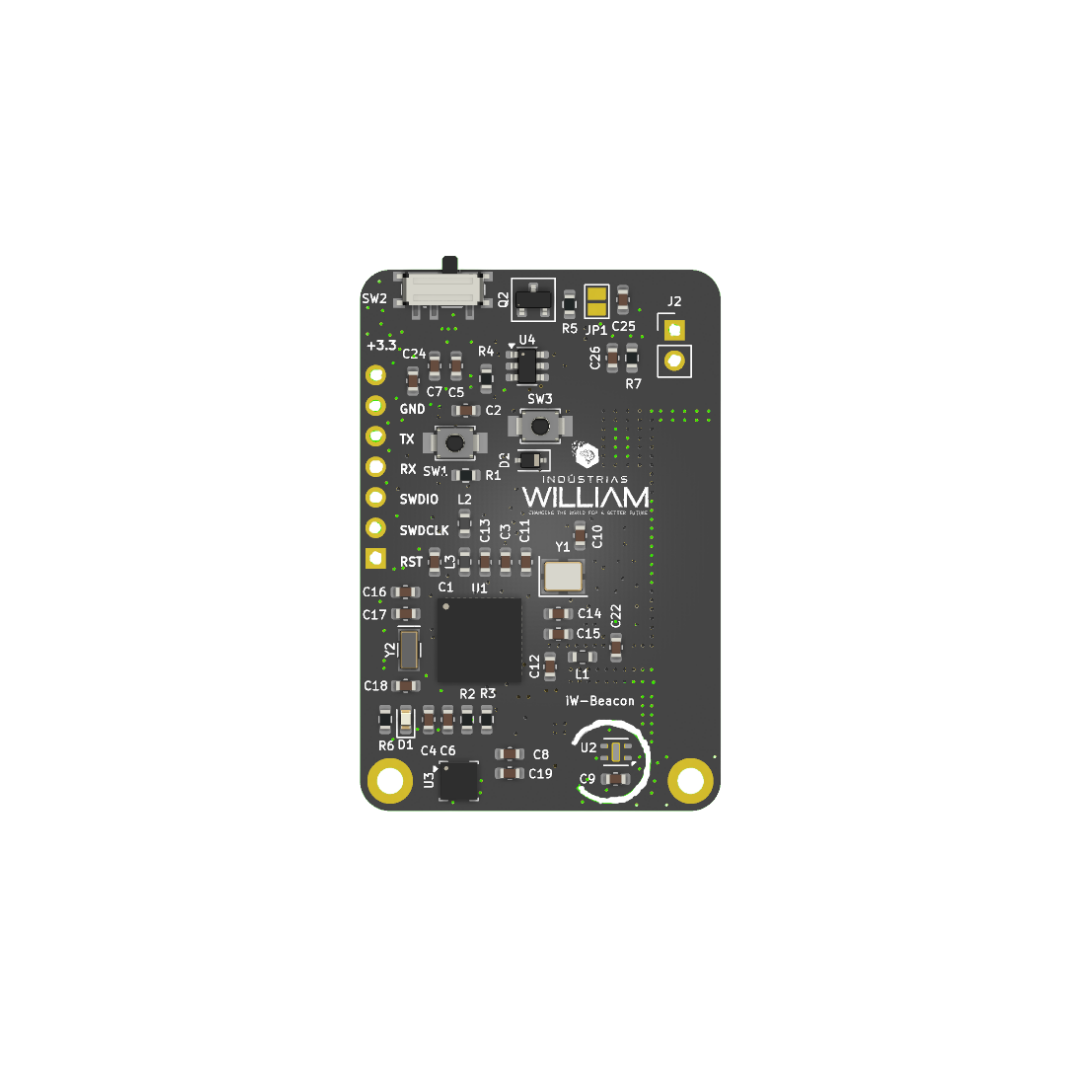
Board overview
The iW-Beacon is organized into four blocks: the nRF52832 radio SoC, the sensors on the I2C bus, the power circuit with the nano-power timer, and the debug interfaces.
3D model
Drag to rotate, scroll to zoom.
Processing and radio — nRF52832
- Nordic
nRF52832SoC (32-bit ARM Cortex-M4F) - Bluetooth 5 Low Energy
- 32 MHz main crystal
- 32.768 kHz crystal for the RTC and low-power timing
- NFC pins available for tap pairing
- internal DC/DC converter (DCC lines) for RF efficiency
The antenna output goes through a matching network (15 nH and 10 uH inductors) to the board antenna.
Integrated sensors
Accelerometer — LIS3DH
An ultra-low-power 3-axis inertial sensor, connected to the SoC over I2C/SPI with interrupt lines (INT1, INT2). Useful to wake the board on motion, and to detect tilt, orientation and tampering.
Temperature and humidity — SHTC3
An SHTC3 sensor (Sensirion) on the I2C bus, with 2.2 k pull-ups. It provides temperature and relative-humidity readings for environmental telemetry directly in the beacon payload.
Both sensors share the same nRF52832 I2C bus, which simplifies the firmware and routing.
Power management (nano-power)
The power circuit was designed for maximum battery life.
BT1battery (coin-cell / battery type) as the primary source- nano-power
TPL5110timer (U4) that sets the wakeup interval AO3401AP-MOSFET load switch (Q2), controlled by the timerJP1jumper to select the power mode- a capacitor bank (47 uF + 4.7 uF + 100 nF) to stabilize transmission peaks
How the cycle works
- The
TPL5110keeps the board off during the programmed interval. - At the end of the interval, it switches the MOSFET on and powers the
nRF52832. - The SoC wakes up, reads the sensors and transmits the BLE packet.
- The firmware signals
DONEto the timer, which cuts power again.
This scheme reduces average consumption to microamperes, since the SoC only draws current during the short transmission window.
Interfaces and debugging
- SWD connector (
J1, 3 ways:SWDCLK,SWDIO,GND) for flashing and debug UART_TX/UART_RXconsole lines- I2C bus shared by the sensors
RESETbutton/line
Electrical characteristics (typical)
| Parameter | Value | Notes |
|---|---|---|
| Logic voltage | 3.3 V | system rail |
| Battery | single cell | coin-cell / battery type (BT1) |
| Load switch | AO3401A | P-MOSFET controlled by the TPL5110 |
| Average consumption | microampere range | dominated by the TPL5110 cycle |
| Crystals | 32 MHz + 32.768 kHz | radio + RTC |
The values above are derived from the schematic components. Actual consumption depends on the transmission interval, the RF power and the active sensors.
Best practices
- program the
TPL5110interval according to the trade-off between data freshness and battery life - use the accelerometer as a trigger for event-driven transmissions
- keep the payload lean to shorten the active radio window
- validate the antenna matching before closing the enclosure